

In 2025, the semiconductor industry is standing at a critical juncture of technological advancement and strategic transformation. From artificial intelligence-led fabrication to green manufacturing and geopolitical supply chain shifts, the sector is no longer just about silicon—it’s about sustainability, sovereignty, and speed. This article explores the latest trends, countrywise investment figures, and the vital role precision machining plays in pushing the boundaries of chip manufacturing.
Miniaturization and Advanced Process Nodes
Miniaturization remains at the core of semiconductor innovation in 2025. The transition to smaller nodes, particularly 3nm and below, is driving demand for ultra-precise manufacturing techniques and tools.
- EUV Lithography, led by ASML’s systems, has become the standard for sub-5nm processes.
- Taiwan’s TSMC has fully transitioned its most advanced facilities to 3nm and is developing 2nm technology for mass production by 2026.
- South Korea’s Samsung Electronics started risk production of its 2nm node in early 2025, with commercial output targeted for 2026.
- Precision machining techniques such as laser ablation, EDM (Electrical Discharge Machining), and ultra-high accuracy CNC systems are now foundational for producing EUV components and advanced photomasks.
AI, Automation, and Smart Factories
AI and machine learning are optimizing every aspect of semiconductor manufacturing—from material selection and process control to predictive maintenance.
- Intel’s factories in the U.S. and Ireland now integrate AI-based defect detection systems that reduce waste by up to 25%.
- Japan’s Renesas Electronics reported a 30% productivity boost after deploying machine learning algorithms for production planning and wafer inspection.
- In China, SMIC (Semiconductor Manufacturing International Corporation) is heavily investing in automation and AI-driven fabs to offset limitations posed by export controls.
Automation extends to equipment calibration, wafer alignment, and even packaging, demanding high-precision mechatronics—where machining tolerances are now measured in sub-micron levels.
Advanced Packaging: A New Frontier
As Moore’s Law plateaus, chipmakers are turning to advanced packaging to increase performance without shrinking transistor sizes.
- Chiplets, 2.5D/3D stacking, and fan-out wafer-level packaging (FOWLP) are being widely adopted.
- AMD and Intel are both using chiplet architecture in new CPU and GPU designs.
- ASE Group in Taiwan and JCET in China are investing more than $1 billion each in 2025 to expand their advanced packaging facilities.
- These innovations require precision-manufactured interposers, ultra-thin substrates, and complex thermal interfaces—highlighting the rising demand for specialized high-precision tooling solutions.
Geopolitical Realignments and Supply Chain Localization
Supply chain disruptions during the pandemic and rising geopolitical tensions, especially between the U.S. and China, have sparked a global movement toward semiconductor self-sufficiency.
- The CHIPS and Science Act in the United States has unlocked $52.7 billion in subsidies for domestic semiconductor manufacturing. Intel, TSMC, and GlobalFoundries are expanding U.S.-based fabs.
- The EU Chips Act allocates €43 billion to bolster Europe’s chip ecosystem. STMicroelectronics and GlobalFoundries are co-developing a new fab in France.
- India’s semiconductor mission, backed by a $10 billion incentive scheme, has seen partnerships like Vedanta-Foxconn and Micron’s packaging plant in Gujarat.
- Japan, supported by a ¥774 billion (~$7 billion) fund, is reviving its domestic semiconductor capability through alliances with TSMC and Rapidus.
Localized production calls for precision engineering vendors and machine builders in each region, creating demand for regional tooling, machining, and component supply chains.
Sustainability and Green Manufacturing
The semiconductor industry is energy-intensive, and sustainability has become a boardroom priority.
- TSMC has committed to using 100% renewable energy by 2050 and aims to cut water consumption by 30% per chip by 2030.
- Intel aims for net-zero greenhouse gas emissions in its global operations by 2040.
- Samsung is investing in carbon capture and ultra-pure water recycling at its Korean fabs.
Green manufacturing necessitates innovations in materials processing, such as low-temperature sintering, eco-friendly wet etching, and dry machining systems. Precision machining partners are now developing low-energy spindles, cryogenic cooling systems, and closed-loop fluid management systems to align with these goals.
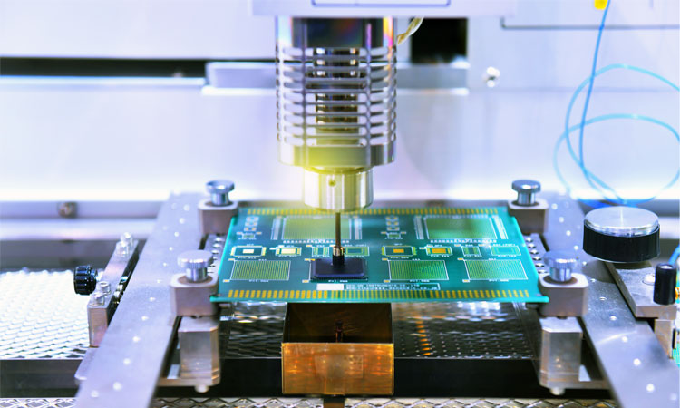
Precision Machining: Silent Hero of the Semiconductor Revolution
Precision machining plays a critical behind-the-scenes role in enabling the semiconductor industry’s transition to future-ready technologies.
- Semiconductor tools, such as lithography stages, mask aligners, and ion implanters, require component tolerances as tight as ±0.5 microns.
- EDM and laser drilling are used for making micron-level vias and high aspect ratio channels in substrates and interconnects.
- Ultra-high precision grinding machines and 5-axis CNC systems are now mandatory for parts used in EUV systems and wafer dicing equipment.
Companies specializing in precision mechanics, advanced tool coatings, and non-contact metrology are seeing massive demand as OEMs raise their quality and reliability requirements.
The 5G-6G Boom and Edge AI Chips
Semiconductor demand is also being driven by massive rollouts of 5G infrastructure and research into 6G communications.
- Qualcomm, MediaTek, and Huawei have launched next-gen 5G chipsets focused on AI at the edge.
- 6G R&D initiatives are gaining traction in South Korea (Samsung), the U.S. (Next G Alliance), and Europe (Hexa-X program).
- These chips require more complex RF front-end modules, SiP (System-in-Package) designs, and higher heat dissipation capacity—all of which rely on novel machining strategies for material shaping and bonding.
Countrywise Highlights – 2025 Semiconductor Snapshot
| Country | Key Investments (2025) | Focus Areas |
| USA | $52.7B (CHIPS Act), $20B Intel Ohio Plant | Localization, AI fabs, advanced packaging |
| Taiwan | $40B TSMC R&D and Fab Expansion | 2nm R&D, EUV, sustainability |
| South Korea | $22B Samsung & SK Hynix expansion | 2nm, memory leadership, 6G |
| China | ~$30B (state-backed, despite sanctions) | Legacy nodes, AI chips, automation |
| Japan | ¥774B (TSMC & Rapidus partnerships) | Sovereignty, advanced packaging |
| India | $10B (Semicon India mission, Micron, Vedanta) | Assembly, packaging, localization |
| EU | €43B (EU Chips Act) | R&D, fabless ecosystem, green manufacturing |