The rapid evolution of electronics is fundamentally changing the way precision components are designed and manufactured. Smartphones are becoming more compact, semiconductor systems more sophisticated, and electronic devices increasingly integrated. Behind this transformation is a manufacturing ecosystem that must deliver complex geometries, smaller features, tighter tolerances and consistent production at scale.
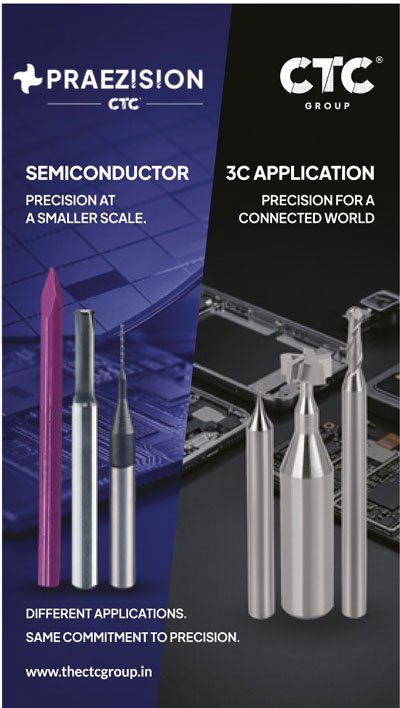
At CTC, we believe precision tooling has an important role to play in enabling this transition. A cutting tool is not simply a consumable in the machining process. Its geometry, substrate, surface technology and consistency can directly influence dimensional accuracy, surface finish, productivity, tool life and process stability.
Our approach to 3C and semiconductor applications therefore begins with a simple principle: start with the application, not the tool.
Precision Beyond Miniaturisation
The 3C sector is characterised by high-volume production and increasingly complex components. Smartphone frames, camera components, connectors, heat sinks and precision structural parts often require machining of aluminium, copper, titanium and advanced engineering materials.
As components become smaller, machining becomes increasingly sensitive to tool performance. CTC’s experience in micro tooling has taught us that the challenge is not simply to manufacture a very small tool, but to manufacture it consistently and repeatably. Our manufacturing processes support rotary tools from 0.030 mm upwards, backed by precision grinding and advanced measurement and inspection systems.
This philosophy becomes particularly relevant in semiconductor applications, where equipment components, fixtures, carriers and other precision parts can involve extremely small features and demanding dimensional requirements. At these scales, runout, edge integrity, vibration, burr formation and surface finish can become critical variables.
Engineering the Complete Tool
We do not believe that there is one tool that is best for every application. Component geometry, machine characteristics, cutting conditions, coolant, required surface finish, cycle time and expected tool life all influence the solution.
Our application and design teams work around these parameters to determine the appropriate combination of geometry, carbide substrate and surface technology. Our portfolio includes ultra-fine-grain carbide tools in uncoated, polished, PVD and CVD-coated configurations.
From Catalogue Products to Application Partnerships
Another important shift we see in the industry is the growing importance of customised tooling. For CTC, special tools have been a core part of our metal-cutting business. Around 70% of our business comes from special tools, reflecting our belief that close engagement with customers often produces better solutions than relying exclusively on standard catalogue products.
Our role is to understand the customer’s machining challenge and work backwards—from the material and component geometry to the machine, cutting conditions and required performance.
India: From a Growing Market to a Manufacturing Base
We see significant potential emerging from India’s growing capabilities in semiconductors, electronics, aerospace, EVs and advanced manufacturing. India’s electronics production has grown from approximately ₹5.54 lakh crore in FY2020-21 to ₹9.52 lakh crore in FY2023-24, while electronics exports more than doubled from ₹1.17 lakh crore to ₹2.41 lakh crore during the same period. Government data indicates electronics production reached approximately ₹12 lakh crore in FY2024-25.
For CTC, India represents both a growing market and an increasingly important manufacturing base from which to serve international customers.
Precision Is a Continuous Journey
CTC’s journey in precision tooling began in 1983 with tungsten carbide tools for the PCB industry. Over four decades, that experience has expanded into micro tooling, industrial cutting tools, specialised applications, in-house R&D, coating technologies and a manufacturing capacity of more than 20 million tools annually.
As 3C and semiconductor manufacturing continue to push the boundaries of miniaturisation and precision, our objective remains consistent: to become more capable, not simply larger.
For us, precision is not a specification achieved at the end of manufacturing. It is a discipline built into tool design, materials, grinding, coating, inspection and application engineering.
As the electronics industry moves towards smaller and more complex components, we believe the future will belong to tooling engineered not just to cut, but to deliver predictable performance at scale.